Stamping technology a core pillar and innovation frontier in connector manufacturing
Share to : 


I.Why is stamping the preferred process for connector manufacturing?
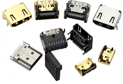
The core components of a connector are pins, terminals, and the housing, typically made of highly conductive and elastic materials such as copper alloys and phosphor bronze. Stamping technology perfectly meets the production requirements of these components due to its unique advantages:
1.High efficiency and high output: High-speed stamping presses combined with progressive dies can produce hundreds or even thousands of parts per minute, meeting the massive market demands of the consumer electronics and automotive industries.
2.Extremely high precision and consistency: Modern precision stamping technology can stably produce terminals with tolerances at the micron level, ensuring the reliability and mating life of each connector contact point.
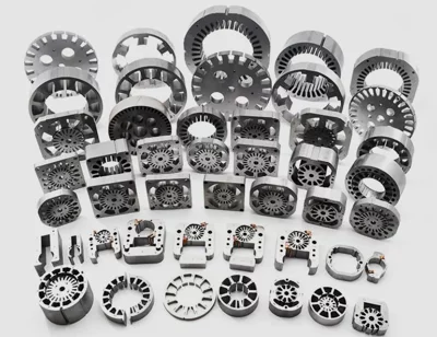
3.Capability to form complex geometries: Stamping not only blanks materials but also, through processes such as bending, rolling, embossing, and finishing, can form terminals with complex three-dimensional structures in a single operation, such as cantilever beam contacts and barbed structures.
4.Excellent material utilization: Through precise layout design, progressive dies can minimize material waste, aligning with the core principles of cost reduction and efficiency improvement in modern manufacturing.
5.Cost-effectiveness: In mass production, the cost per unit is reduced to an extremely low level, which is difficult to match by other processing methods (such as CNC machining and MIM).
II. Key Technologies and Challenges in Connector Stamping
Although stamping is a mature technology, its technical challenges are becoming increasingly severe as connectors develop towards being "smaller, lighter, and faster".
Miniaturization and high precision:
- Challenge: As connector pitch evolves from 1.0mm to 0.3mm or even smaller, the size and tolerance requirements of the terminals have reached their limits.
- Technical solutions: Require ultra-high precision molds (usually made of tungsten steel), stable high-precision stamping equipment (such as servo presses), and strict in-process quality control (such as vision inspection systems).
Applications of high-strength thin materials:
- Challenge: To meet the requirements of high mating cycles and high contact force, connector manufacturers began to use higher strength copper alloys, but these materials are more difficult to stamp and cause more wear on the molds.
- Technical solutions: Use raw materials with surface lubrication, optimize mold clearance design, and use high-quality coatings (such as TiCN, Diamond-like Carbon) to extend mold life.
Integrated composite process:
- Trend: To further improve efficiency and performance, stamping is no longer just about "punching" and "pressing." Integrated stamping and electroplating is becoming an important trend. Integrating electroplating stations into progressive dies allows for immediate partial or overall electroplating (such as gold or tin plating) after stamping, reducing production steps and improving quality consistency.
III. Future Trends in Stamped Connector Manufacturing
Intelligentization and Digitalization:
- Utilizing IoT technology, real-time monitoring of stamping equipment parameters such as tonnage, vibration, and temperature enables predictive maintenance and reduces unplanned downtime.
- Through big data analysis, stamping process parameters are optimized to achieve root cause tracing and proactive prevention of quality issues.
Integration of New Materials and Processes:
- For automotive high-voltage connectors, stamping processes need to handle thicker sheet metal and different metal materials.
- Deep integration with insert injection molding allows for the direct embedding of stamped precision terminals into plastic molds, creating a complete connector housing assembly in a single step.
Ultra-precision and Micro/Nano Manufacturing:
- For ultra-miniature connectors used in medical devices and high-end wearable devices, stamping technology is being combined with etching, laser processing, and other processes to expand into the field of micro/nano manufacturing.
Green and Sustainable Development: Optimize waste sorting to reduce waste and establish an efficient waste recycling system.
- Develop environmentally friendly downstream processes such as cyanide-free electroplating and low-precious metal electroplating, and integrate them with the stamping process to achieve green manufacturing.
In conclusion
Stamping, a seemingly traditional manufacturing technology, is constantly being infused with new technological elements in the dynamic field of connectors. It is not only the cornerstone of large-scale, low-cost production, but also a key engine driving connector technology towards miniaturization and high performance. For stamping companies and connector manufacturers, continuous investment in precision mold technology, intelligent manufacturing, and the integration of innovative processes is an inevitable choice to maintain a leading position in future market competition.
With years of hands-on experience, I have honed my skills in navigating the complexities of global commerce, offering invaluable insights and solutions to address customer needs. My commitment to excellence and dedication to customer satisfaction ensure that I deliver exceptional service, guiding clients through every step of the trading process with confidence and proficiency.
Related Topics:
connectorYou may also like
Related News
Real situation of Rerain roller feeder
Oct 31, 2023
Miss He from PATEC Visits Chainmorn
Oct 31, 2023